GLASS CORE TECHNOLOGY
Contact [email protected] for assistance with your next generation microelectronics needs.
ULTRA-MINIATURIZED | HIGHLY INTEGRATED | HIGH PERFORMANCE
THROUGH-GLASS VIAS (TGVs) IN GLASS SUBSTRATES
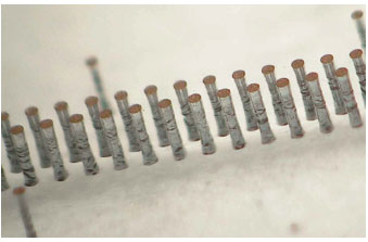
The industry’s only proven process for metalization and hermetic sealing of ultra-high-density Through-Glass Vias (TGVs) enables:
- Extreme Miniaturization & Integration
- High Performance Electronics
- High Reliability Packaging Solutions
REDISTRIBUTION LAYER (RDL) CIRCUIT PATTERNING ON GLASS
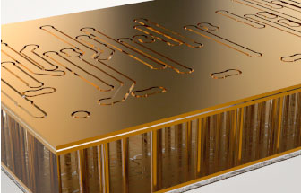
RDL’s unique thin-film process enables circuit formation on glass substrates, providing for:
- Low Loss Fan-Out of Chip and Package Interconnects
- Lower Cost Compared to Traditional Silicon-Based Interposers
- Integrated Passive Devices, Filters
- Endless IoT Applications
HIGH PERFORMANCE ELECTRONICS
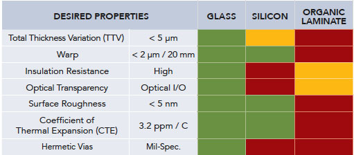
Glass substrates offer high structural integrity, resistance to vibration and temperature, environmental ruggedness, and low electrical loss, making them ideal for next generation microelectronics demands. Samtec’s proprietary Glass Core Technology process leverages the performance benefits of glass to enable performance optimized, ultra-miniaturized substrates for next generation designs.
Automotive MEMS and Sensors
Smart Building Sensor Modules
Medical Robotics Sensors
RF Component and Modules
Advanced RF SiP
Automotive RF
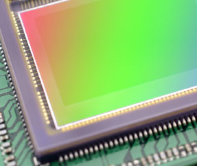
CMOS Image Sensor (CIS)
Automotive Camera Modules
Active Images & LiDAR
Solid State Medical Images
GLASS CORE TECHNOLOGY DESIGN RULES & GUIDELINES
NOTE:
These dimensions are guidelines designed to help release product to manufacturing as quickly as possible. Full capabilities are not limited to the specifications listed below. Please contact [email protected] for applications with tighter requirements.
THROUGH-GLASS VIA (TGV) ENABLED GLASS INTERPOSERS
Samtec’s Through-Glass Vias (TGVs) enable Glass Core Technology (i.e., glass interposers, smart glass substrates and microstructured glass substrates). TGV-enabled glass substrates permit the integration of glass and metal into a single wafer, while interposers promote more efficient package interconnects and manufacturing cycle times.
The hermetically sealed TGVs are manufactured from both high quality borosilicate glass, fused silica (aka quartz), and sapphire. Through the use of high quality glass wafer material, combined with advanced interconnect technologies (e.g., Redistribution Layer), Samtec’s Glass Core Technology enables a one-of-a-kind packaging product.
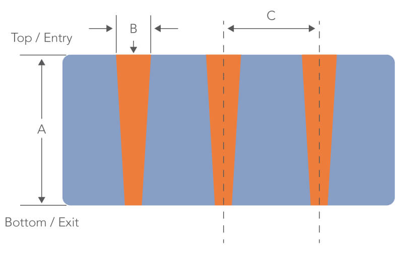
| Through-Glass Via Cross-Section View |
|---|
 |
|
Glass Characteristics & Applications
|
|---|
|
Borosilicate Glass
Fused Silica
|
| Detail | UNITS | |
|---|---|---|
| A | Nominal Glass Thickness | 260 µm |
| B | Via Diameter (min) | 40 µm |
| Via Tapering | 5 deg | |
| C | Via Pitch | 2 x Via Diameter |
| Total Thickness Variation (TTV) | 15 µm | |
| Via Positional Accuracy | +/- 5 µm |
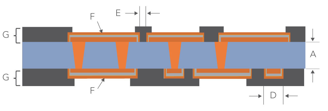
REDISTRIBUTION LAYER (RDL) TECHNOLOGY
Samtec's Redistribution Layer (RDL) technology enables circuit formation on glass substrates for interfacing to TGVs via a unique thin-film approach. This provides for low loss fan-out of chip and package interconnects, and lower costs compared to traditional Silicon-based interposers.
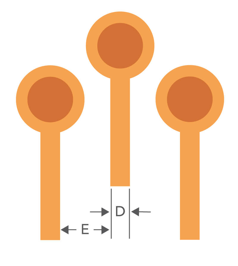
| Specifications | Current | Roadmap | |
|---|---|---|---|
| No. of Metal Layers per Side | 2 | 4 | |
| A | Glass Core Thickness | 260 µm | 100 - 450 µm |
| Via Diameter | 40 µm | 10 µm | |
| Annular Ring (Catch Pad) | 20 µm larger than Via Diameter | ||
| Via Pitch (min) | 2 x Diameter | 40 µm | |
| D, E | Line/Spacing (min) | 15 µm / 15 µm | 10 µm / 10 µm |
| F | Copper Thickness | 1 - 5 µm | |
| G | Dielectric Thickness 1 & 2 (min) | 4 µm | |
| Solder Ball Types | SN63Pb37 and SAC305 | Pb95Sn5, Pb90Sn10, Cu/Sn Pillars | |
| Under Bump Metallization (UBM) | ENIG | ENIPIG |
| Top View of Circuit for Top/Bottom RDL |
|---|
 |
| Cross-Section - 2 Metal Layers (Current Capability) |
|---|
 |
| Cross-Section - 4 Metal Layers (Future Capability) |
|---|
-cross-section.jpg) |
Visit samtec.com/microelectronics to learn more about Samtec's Glass Core Technology and Advanced IC Packaging Capabilities. Contact [email protected] to speak with our specialists about your next generation microelectronics needs.