MICROELECTRONICS
INTERCONNECT SOLUTIONS
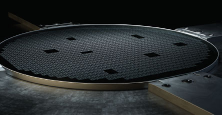
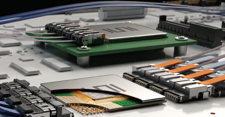
Next generation microelectronics require increased performance and integration, advanced chip technology and miniaturization.
Samtec’s extensive microelectronics and high-speed interconnect expertise, along with our proven methods for package integration, miniaturization, wafer level processing and signal integrity optimization, enable us to provide a unique level of support for advanced microelectronics applications.

© 2024 Samtec. All rights reserved.
 Your Privacy Choices